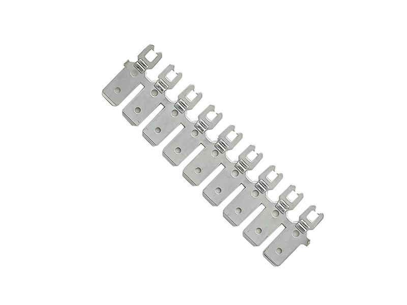
Strong conductivity stamping lead frame
Product
DESCRIPTION
Specifciation of Strong conductivity stamping lead frame:
★ The raw material for lead frame is Copper-zinc alloy. The product is electroplated using raw materials,with copper as the base and then matte tin plating. product needs to be stamped. The thickness is 0.3mm.
★ For mechanical properties, lead frames need to be tinned after stamping.
★ The lead frame is a thin metal frame to which semiconductor is attached during package assembly. The quality of the lead frame is critical: any minor defect can seriously compromise the performance and reliability of the final IC device.
★ No pollution to environment. Part complies with RoHS.
★ The stamping speed is around 400 times/ min.
★The product is subjected to a minimum of 8 hours of salt spray testing
At Dogguan Fortuna, we can customize progressive dies for such parts according to customer requirements and drawing parameters. We spare no effort to meet high speed production and provide our customers with quality quantities.
Parameter of Strong conductivity stamping lead frame | |||
Place of Origin | Guangdong, China (Mainland) | Application | electronics |
Material | H65 | Surfacetreatment | tin plating |
Size | 35*25*18mm | Usage | connecting |
Color | sliver | Special | OEM/ODM is welcome |
Certificate | IATF16949 ISO14001 SGS RoHS | Other | N/A |
Packaging & Delivery | |||
Single package size | 55*48*35 cm | Package Type | Plastic tray and exported carton |
Single gross weight | 9 kg | Lead Time | 15 days |
PRODUCT ADVANTAGES
Description and advantage of Strong conductivity stamping lead frame
QUALITY CONTROL
Our quality team uses high-precision instruments to inspect the product every hour to meet the accuracy and yield requirements of the product.
PACKING
Based on the product's structural process, product weight, shipping requirements and customer requirements, our process engineers will evaluate the right packaging solutions for the product, which are fully compliant with all shipping conditions and modes of transport. The main packaging methods include bulk packaging, plastic pallet packaging, carrier tape packaging and reel packaging.
welcome to discuss
your next project.


