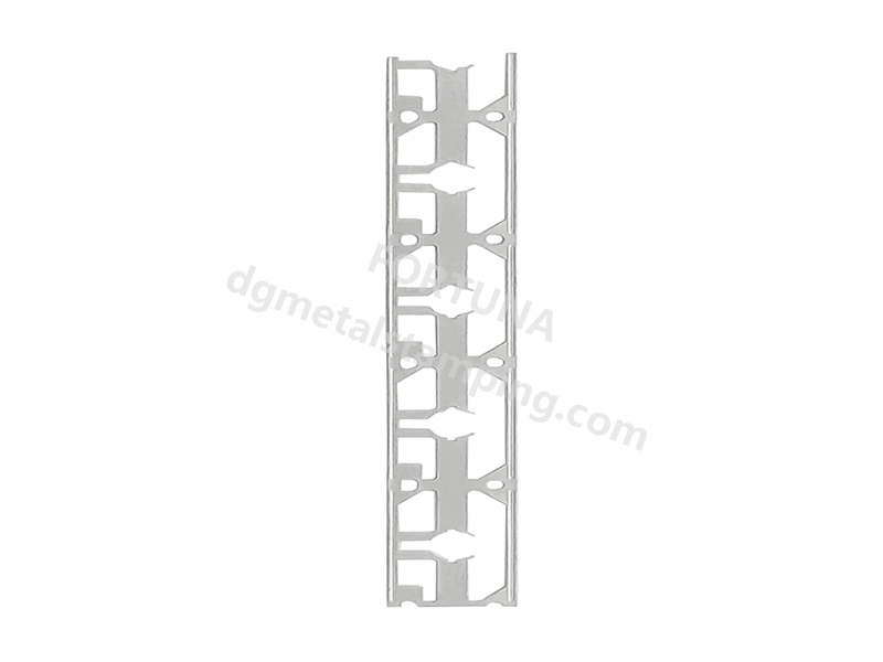
Tinned-plating precision stamped lead frame
Product
DESCRIPTION
Specifciation of Tinned-plating precision stamped lead frame:
★ Gennerally, The raw material for lead frame is C5191 with excellent electrical conductivity.The product needs to be stamped before plating.The thickness is 0.30mm.
★ The lead frame also needs to be tinned on the surface to maintain the stability of the contact between electronic components.
★ The lead frame is a thin metal frame to which the semiconductor is attached during package assembly. The quality of the lead frame is critical: any minor defect can seriously compromise the performance and reliability of the final IC device.
★ No pollution to environment. Part complies with RoHS.
★ The stamping speed is around 300-500 times/ min.
At Dogguan Fortuna, Products are widely used in home appliance, communication equipment, auto parts, new energy vehicles and aviation filed. Product quality and affordable price won the praise of customers. Products are exported to Japan, USA, Germany, the Czech Republic, Hungary, Norway and other countries.
PRODUCT PARAMETERS
Parameter of Tinned-plating precision stamped lead frame | |||
Place of Origin | Guangdong, China (Mainland) | Application | Consumer electronics |
Material | C5191 | Surfacetreatment | tin plating |
Size | 45*38*25mm | Usage | touching |
Color | sliver color | Special | OEM/ODM is welcome |
Certificate | IATF16949 ISO14001 SGS RoHS | Other | N/A |
Packaging & Delivery | |||
Single package size | 55*48*35 cm | Package Type | Plastic tray and exported carton |
Single gross weight | 8 kg | Lead Time | 15 days |
PRODUCT ADVANTAGES
Description and advantage of Tinned-plating precision stamped lead frame
QUALITY CONTROL
Our quality team uses high-precision instruments to inspect the product every hour to meet the accuracy and yield requirements of the product.
PACKING
Based on the product's structural process, product weight, shipping requirements and customer requirements, our process engineers will evaluate the right packaging solutions for the product, which are fully compliant with all shipping conditions and modes of transport. The main packaging methods include bulk packaging, plastic pallet packaging, carrier tape packaging and reel packaging.
welcome to discuss
your next project.


